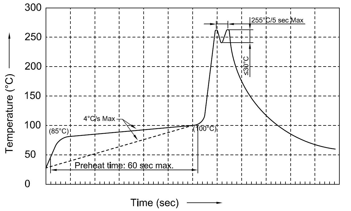
·Recommended Wave Soldering Profiles:
Notes:
1.Recommend pre-heat temperature of 105℃ or less (as measured with a thermocouple
attached to the LED pins) prior to immersion in the solder wave with a maximum solder bath
temperature of 260℃.
2.Peak wave soldering temperature between 245-255℃ for 3 sec (5 sec max).
3.Do not apply stress to the epoxy resin while the temperature is above 85℃.
4.Fixtures should not apply stress on the component when mounting and soldering process.
More than one wave soldering is not allowed.
·Terms and conditions for the usage of this document
1. The information included in this document reflects representative usage scenarios and intended for technical reference only.
2. The part number, type, and specifications mentioned in this document are subject to future change and improvement without notice. Before production usage customer should refer to the latest datasheet for the updated specifications.
3. When using the products referenced in this document, please make sure the product is being operated within the environmental and electrical limits specified in the datasheet. If customer usage exceeds the specified limits, LITEKEY will not be responsible for any subsequent issues.
The information in this document applies to typical usage in consumer electronics applications. If customer’s application has special reliability requirements or have life-threatening liabilities, such as automotive or medical usage, please consult with LITEKEY representative for further assistance.
1.Storage conditions:
a. Prevent continued exposure to the condensing moisture environment and keep the product away from rapid transitions in ambient temperature.
b. LEDs should be stored with temperature ≤30℃ and relative humidity ≤60%。
c. Product in the original sealed package is recommended to be assembled within 72 hours of opening. Product in opened package for more than a week should be baked for 30 (+10/-0) hours at 85-100℃.
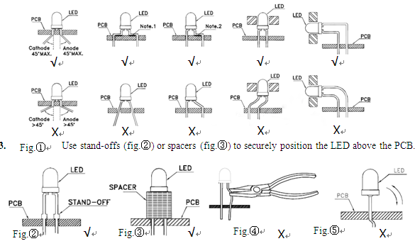 2. The lead pitch of the LED must match the pitch of the mounting holes on the PCB during component. Lead-forming may be required to insure the lead pitch matches the pitch. Refer to the figure below for proper lead forming procedures. (Fig.①)
4. During lead forming, use tools or jigs to hold the leads securely so that the bending force will not be transmitted to the LED lens and its internal structures. Do not perform lead forming once the component has been mounted onto the PCB.(fig.④)
5. Do not bend the leads more than twice. (fig.⑤)
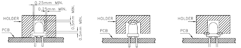
6. During soldering, component covers and holders should leave clearance to avoid placing damaging stress on the LED during soldering
7. Through-hole LEDs are incompatible with reflow soldering.
8. Cleaning:
a. At room temperature, cleaning should occur only with isopropyl alcohol for a duration of no more than one minute when necessary. Dry at room temperature before use.
b. Do not clean the LEDs by the ultrasonic. When it is absolutely necessary, the influence of ultrasonic cleaning on the LEDs depends on factors such ultrasonic power and the assembled condition. Ultrasonic cleaning shall be pre-qualified to ensure this will not cause damage to the LED.
9. Other:
a. Above specification may be changed without notice. LITEKEY will reserve authority on material change for above specification.
b. When using this product, please abserve the absolute maximum ratings and the instructions for using outlined in these specification sheets. LITEKEY assumes no responsibility for any damage resulting from use of the product which does not comply with the absolute maximum ratings and the instructions included in these specification sheets.
These specification sheets include materials protected under copyright of LITEKEY COMPANY LIMITED. Please don’t reproduce cause by anyone to reproduce them without LITEKEY’s consent.
 English


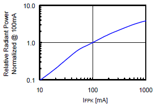
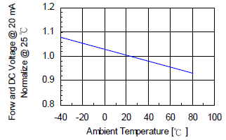
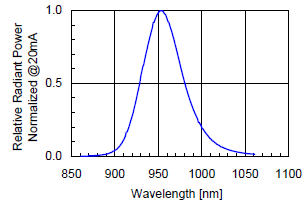 FIG. 1 Forward Current Vs. Forward Voltage FIG. 2 Relative Radiant Vs. Wavelength